Gallium oxide (Ga2O3) is an emerging ultra−wide bandgap semiconductor with a bandgap of 4.5–5.3 eV [[1], [2], [3], [4], [5], [6], [7], [8]], a better breakdown electric field, and an excellent Baliga's figure−of−merit (BFOM) than the other semiconductor materials, like SiC [9] and GaN [10]. Table 1 summarizes the main parameters of β–Ga2O3, as compared with other semiconductor materials, including Si, GaAs, SiC, GaN, diamond, and AlN. β–Ga2O3 shows a higher bandgap with the value rage from 4.5 to 4.9 eV, which higher than that of SiC (3.3 eV) and GaN (3.4–3.6 eV), leading to a higher resistance to high temperature and radiation properties. Breakdown field (8 MV/cm), as one of the important parameters for semiconductors, allows β–Ga2O3 materials to withstand high voltage in power devices. With about ~3443 BFOM for Ga2O3, which far more than SiC, GaN, and AIN, helps minimizing the conduction losses in power devices. All these excellent characteristics contribute to the properties of a higher temperature tolerance, a better resistance to radiation and a lower conductive loss, resulting in its widely applications in power electronics [[11], [12], [13], [14], [15], [16], [17], [18], [19], [20], [21], [22], [23], [24], [25], [26]], UV − blind photodetectors [[27], [28], [29], [30], [31], [32], [33], [34], [35], [36], [37], [38]], solar cells [[39], [40], [41], [42], [43], [44], [45]], gas sensors [[46], [47], [48], [49], [50], [51], [52], [53], [54]], light–emitting diode (LED) [[55], [56], [57], [58], [59], [60], [61], [62], [63]], photocatalyst [[64], [65], [66], [67], [68], [69], [70], [71], [72], [73]] and so on. Moreover, due to its better radiation stability properties, Ga2O3 was proved to be a potential material utilized in high–radiation environment [[74], [75], [76], [77], [78], [79], [80], [81], [82], [83], [84]]. In recent years, owing to the advantages of its excellent performance and broad application prospects in semiconductor technology, Ga2O3 materials have attracted extensive academic and technological attention.
There are five different polymorphs of Ga2O3 which known as α − Ga2O3 (rhombohedral), β − Ga2O3 (monoclinic), γ − Ga2O3 (defective spinel), δ − Ga2O3 (cubic), and ε − Ga2O3 (orthorhombic) (Table 2). Among the five polymorphs, both α − Ga2O3 and β − Ga2O3 are the most common polymorphs and have attracted most of the recent attentions. The β − Ga2O3 is the thermodynamically stable polymorph under normal conditions of temperature and pressure, and the other four polymorphs can be converted into β − Ga2O3 when they are heated to a certain temperature [[111], [112]] (Fig. 1). Because of that the melting point of β − Ga2O3 nearly reach up to about 1800 °C [113], it becomes the only single−crystal phase that can be grown with low−cost melt−grown methods at high temperatures. α − Ga2O3 is known as the metastable phase, but it is also in the limelight due to its highest bandgap of about 5.1–5.3 eV [[114], [115], [116]], which is highly beneficial for the advancement of high−performance power devices [[117], [118], [119]]. Phase−pure α − Ga2O3 can be prepared from precursors during 350–600 °C [[120], [121]], and then transforms into β − Ga2O3 at the 600 °C above [122]. Compared with β − Ga2O3, ε − Ga2O3 is the second most stable phase of Ga2O3 with strong ferroelectric behavior and large polarization, making it promising for applications both in electronic and piezoelectric devices [[123], [124]]. γ − Ga2O3 was reported to present excellent photocatalyst and luminescent properties [[125], [126], [127]] because of its defective spinel structure containing both gallium and oxygen vacancies. Few studies have been reported on the synthesis and application of δ − Ga2O3 due to their low thermal stability [128].
High quality of Ga2O3 materials is the prerequisite to achieve excellent performance. In order to meet the needs of the electrical devices and other applications concerned, the powder materials synthesis technologies play a significant role in improving the quality of Ga2O3 powder materials. The main preparation methods for Ga2O3 nanomaterials or films based on the phase classification are divided into gas phase synthesis method and liquid phase synthesis method. The gas phase synthesis method contains physical vapor deposition (PVD) techniques (including RF magnetron sputtering (EFMS) [[143], [144], [145]]; pulsed laser deposition (PLD) [[146], [147], [148]], and molecular beam epitaxy (MBE) [[149], [150], [151]]) and chemical vapor deposition (CVD) techniques (including metal–organic chemical vapor deposition (MOCVD [[152], [153], [154], [155], [156], [157], [158], [159]]); hydride vapor phase epitaxy (HVPE) [[160], [161], [162], [163], [164]]; plasma–enhanced chemical vapor deposition (PECVD) [[165], [166], [167]]; mist chemical–vapor deposition (Mist–CVD) [[168], [169], [170], [171], [172]]; atomic layer deposition (ALD) [[173], [174], [175], [176]] and so on. These CVD techniques can be classified into cold-wall and hot-wall CVD based on the heating source concentrated in the substrate or the entire reaction chamber. Hot-wall CVD consists of most of MOCVD [[152], [153], [154], [155]], HVPE [[160], [161], [162]], and Mist-CVD [[168], [169], [170], [171]] which employing hot reactors, meanwhile, cold-wall CVD are comprised of these techniques using cold reactors [[156], [157], [158], [159],163,164,172], PECVD and ALD.). Benefit from the precision equipment structure and complex process for these methods, the technologies, such as MOCVD, MBE, and HVPE, are usually used for high–quality epitaxial growth of Ga2O3 films and nanomaterials. MOCVD is a relatively mature epitaxial growth method in the semiconductor industry today. Due to this technology can grow a large area of Ga2O3 film with high growth rate and low film defects, making it to be a suitable for industrial production. Thanks to the fast growth rate and simple process, HVPE has been a promising approach for Ga2O3 film growth, however, the issues of surface roughness and defects remains. MBE shows its significant advantages on lower defects and residual carrier concentration, but the low deposition rate and high equipment cost limit its application. Compared with the technologies mentioned above which need complex equipment and high energy consumption, liquid phase synthesis undoubtedly greatly reduces the energy consumption and cost in the production process. It is common to use liquid−phase synthesis method to produce Ga2O3 powder materials, because this method can produce high purity and fine−grained powders with simple operation, low cost, and mass production efficiency. The liquid−phase synthesis routes of nanoparticles including electrodeposition, direct−precipitation, chemical bath deposition, hydrothermal and solvothermal synthesis, sol−gel, forced hydrolysis, colloidal synthesis, hot−injection synthesis methods and so on [177,178]. In this paper, we are aim to discuss the effects of synthesis methods and conditions on the morphology and size of Ga2O3 particles and its applications, in order to provide a suitable synthesis method and applications for Ga2O3 particles with controllable morphology and size.


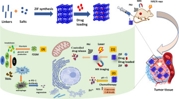
留言 (0)