
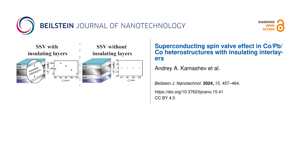
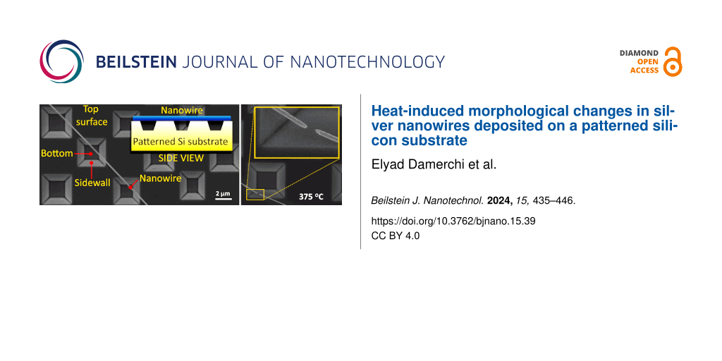
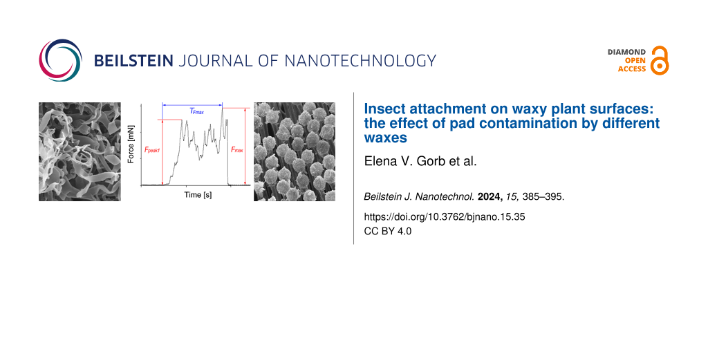
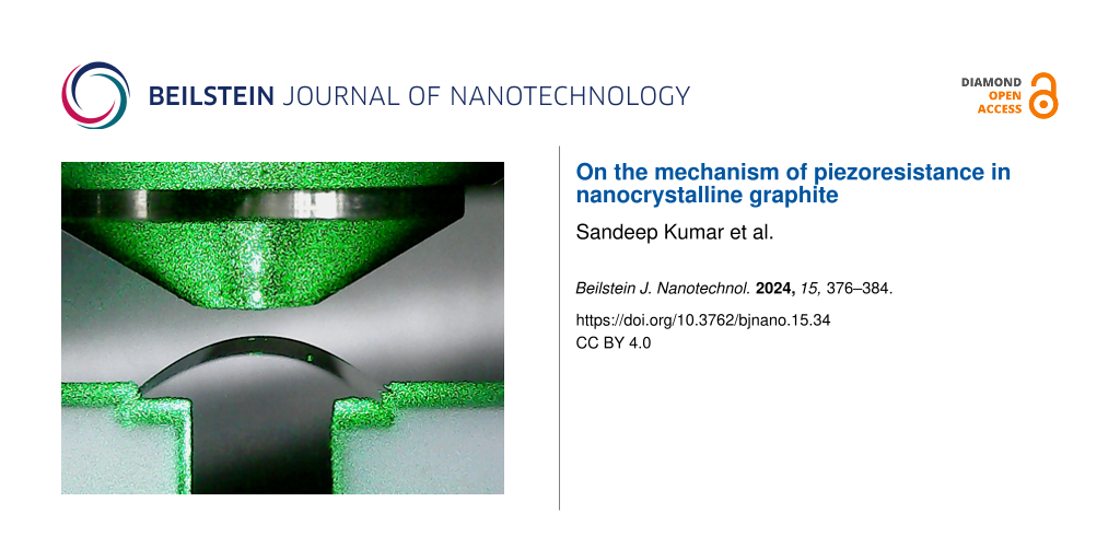
記住我


The advent of two-dimensional (2D) layered materials beyond graphene has initiated a new field of research . In the family of 2D layered structures, transition metal dichalcogenides (TMDs) have attracted considerable attention from academia and regarding potential applications because of a number of remarkable properties . Particularly, it was found that the properties of layered TMDs drastically change when their thickness is reduced to a monolayer . Layered TMD structures have a graphite-like structure with each graphene sheet replaced with an X–M–X or MX2 triatomic layer, where X is a chalcogen atom (e.g., sulfur, selenium, or tellurium) and M is a transition metal atom (e.g., molybdenum or tungsten) .
Among the layered TMD materials, molybdenum disulfide, MoS2, is of particular interest in optoelectronic applications because of its transition to a direct bandgap semiconductor with very high photoluminescence quantum yield when thinned down to a monolayer . Its unique electronic and optical properties could provide an edge in many future applications.
The multilayers MoS2 structures are of the most common 2Hc type, where atomic layers are arranged in such way that the stacking between two adjacent layers corresponds to a twist angle of θ = 60°, and any Mo atom is sitting on top of two S atoms of the adjacent layers . However, during the synthesis process (e.g., chemical vapor deposition (CVD) synthesis) or when using precise transfer or AFM tip manipulation techniques , twisted MoS2 can be formed with two adjacent layers stacked with a relative twist angle (θ) varying from 0 to 60°. Such twisted-layered MoS2 structures can exhibit a variety of interesting physical properties including unconventional super conductivity , non-linear optics , and moiré excitons .
Because the properties of MoS2 flakes are first a function of their thickness, or layer number (N), it is of a primary importance to determine the N of MoS2 flakes, including twisted MoS2 flakes and defective MoS2 flakes, synthesized by different ways. Independently of the structural organization between adjacent layers, a MoS2 flake is usually named NL-MoS2, or simply NL, with N being the number of MoS2 triatomic layers, which defines the thickness of the flake.
Several optical techniques have been developed to identify the N of MoS2 flakes produced by different methods. Among these techniques, Raman spectroscopy is widely used thanks to its convenience, non-destructiveness, and sensitivity to materials change, including strain, temperature, doping, and defects . Concerning the characterization of MoS2 flakes, different information can be derived from the measurement of the Raman features (frequencies, linewidths, and intensities) of intralayer phonon modes as well as those of the interlayer modes, the so-called layer breathing (LB) modes and shear (S) modes.
Recently, we have developed the reproducible direct growth of wafer-scale MoS2 thin films on SiO2/Si substrates by direct liquid injection pulsed-pressure chemical vapor deposition (DLI-PP-CVD) using low-toxicity precursors . Such MoS2 thin films showed good stoichiometry (Mo/S = 1.94–1.95) and the potential for high photoluminescence quantum yield. However, atomic force microscopy revealed that they are constituted of nanoflakes (with a lateral size of typically 50 nm) with possibly a distribution of thicknesses. Furthermore, depending on the synthesis conditions, the MoS2 surface coverage can be incomplete, and the thin film average thickness can vary. These samples thus have characteristics, especially thickness inhomogeneities smaller than the laser spot size, that differ from the ones used to establish Raman spectroscopy-based MoS2 layer counting methods . In this context, the primary purpose of this work is to develop and validate an approach for determining the average thickness of such sub-laser spot size inhomogeneous MoS2 thin films using Raman spectroscopy.
First, we reassess here as a ground work the information that can be derived from the Raman spectra of MoS2 flakes for the evaluation of their thickness, N. Different Raman criteria for the determination of the thicknesses of MoS2 flakes are first recollected; after the specification of the experimental protocol, domains and limits of application of these criteria are precisely defined from measurements performed on reference samples. These samples are well-characterized, either mechanically exfoliated or standard CVD MoS2 large flakes deposited on 90 ± 6 nm SiO2 on Si substrates. Then, we determine which Raman information is relevant to estimate the average thickness of MoS2 samples produced by the DLI-PP-CVD method, which are constituted of nanoflakes and, thus, significantly different from the reference samples. Finally, an original procedure based on the layer breathing mode intensities is proposed to evaluate the surface coverage for each N, that is, the ratio between the surface covered by exactly N layers and the total surface, in DLI-PP-CVD samples.
Results and Discussion Experimental procedureTo define a robust experimental Raman protocol to evaluate the thickness of a MoS2 flake (i.e., its number of layers, N), it is first necessary to specify some parameters that can have a direct influence on the quality and accuracy of the results. The first parameter is the wavelength of the incident laser light used in the Raman experiments. As it will be detailed in the following, the measurements of the frequencies, linewidths, and intensity of first-order Raman active phonon modes of MoS2 have to be obtained with good accuracy in order to evaluate the thickness of a MoS2 flake. These phonons modes are (i) the in-plane phonon mode involving relative motion of Mo and S atoms with E′ symmetry for a monolayer (E12g for bulk) and (ii) the out-of-plane phonon mode involving only out-of-plane motions of S atoms with A′1 symmetry for a monolayer (A1g for bulk). These modes are located around 385 and 405 cm−1, respectively, in neutral and defect-free MoS2 monolayers . More precisely, in MoS2 multilayers, the symmetries of these phonon modes are E′ and A′1 for an odd number of layers, and Eg and A1g for an even number of layers. For simplicity, hereafter when we will discuss the dependence on N of the features of these phonon modes, they will be simply referred to as in the bulk, E12g and A1g, independently of the number of layers.
A drastic change of the Raman spectra, especially in the frequency range of the A1g and E12g modes, occurs when the spectra are excited at an energy close to those of the A and B excitons located around 655 nm (1.89 eV) and 601 nm (2.06 eV), respectively, in MoS2 monolayers . When the incident laser energy is in the range of the A and B exciton energies (the so-called resonance conditions), other bands associated to different second-order processes are observed in the Raman spectra with a strong intensity, their frequencies, widths, and intensity depending on the excitation energy . In addition, resonance conditions alter the symmetry selection rules of phonons of MoS2. Some of the second-order bands overlap with the A1g and E12g modes, complicating the exact determination of the parameters of these modes recorded under resonance conditions. Furthermore, since the MoS2 exciton characteristics (energy, width, and spectral weight) can be changed by several factors (e.g., stacking, strain, doping, and defects), the Raman intensities measured with a single laser wavelength close to exciton energies can be affected by external factors and differ for samples elaborated by different methods. For these reasons and in the aim to use Raman spectroscopy to count the number of MoS2 layers, one must necessarily work under off-resonance conditions, that is, by using incident laser energy far from both exciton resonance energies. In this work, we chose to perform Raman experiments using 532 nm (2.33 eV) laser excitation, because this is sufficiently far from the energy range of A and B excitons .
All Raman spectra reported in this paper were recorded on different samples deposited on SiO2/Si(100) substrate. Hence, the second parameter essential to define is the SiO2 thickness. Indeed, the multiple reflection interferences that occur in the air/MoS2/SiO2/Si structure influence significantly the intensity of the phonon modes . In this work, we chose to focus on substrates with a SiO2 thickness around 90 nm, which corresponds to the first optimum value for MoS2 monolayer (N = 1) Raman enhancement with a 532 nm excitation energy and also amplifies the signal in the wavelength range of photoluminescence emission (around 650 nm).
The third parameter to define is the power of the 532 nm light, Pλ, impinging the sample. Much of the Raman information available to evaluate the thickness of MoS2 flakes is based on the following parameters: (i) on precise measurements of frequency of the A1g and E12g phonon modes of MoS2. These lead to a precise knowledge of the frequency difference ΔωA−E. It was established that ΔωA−E depends monotonously on the number of layers, and ΔωA−E is largely used as criterion to evaluate the thickness of MoS2 flakes ; (ii) on the precise evaluation of the integrated intensities of the phonon modes of MoS2, namely A(A1g) and A(E12g), with respect to the integrated intensity of the 521 cm−1 mode from a bare area of the oxidized silicon substrate, A0(Si), used as an intensity reference , or from the silicon substrate underneath the MoS2 flake, A2D(Si) ; (iii) on the precise measurement of the A2D(Si)/A0(Si) intensity ratio ; and (iv) on the measurement of ultralow-frequency modes, the so-called breathing modes and shear modes. The frequencies and the number of LB and S modes allow one to identify the number of layers and the presence of twist between adjacent layers from the vanishing of the S modes in twisted MoS2 flakes .
Then, it is essential to determine the limit value of the laser power so that the above measurements are not affected by laser irradiation. Figure 1 shows the evaluation of the temperature of MoS2 flakes prepared in different ways and that of the Si substrate as functions of the laser power impinging on the sample through a 100× objective (N.A. 0.9). The power was cycled between ≈5 μW and ≈2 mW. The temperature of MoS2 flakes is evaluated from the Stokes/anti-Stokes intensity ratio of A1g phonon modes (similar results are obtained using E12g) and that of silicon from the Stokes/anti-Stokes intensity ratio of the 521 cm−1 Si mode (see for method details). While the silicon temperature is quasi-insensitive to Pλ, the temperature of MoS2 flakes changes monotonically, reversibly, and quasi-linearly with Pλ (see inset of Figure 1). For MoS2, we found an increase rate of 25–30 °C/mW for monolayers (1L-MoS2) and 40–45 °C/mW for bilayers (2L-MoS2). Usual effects of sample heating are the frequency shift of the phonon modes and their concomitant broadening. In Supporting Information File 1, the frequency and the linewidth of the Si mode as functions of the laser power are displayed (Figure S2). These two parameters are found to be insensitive to Pλ below 0.5 mW. More intriguing is the evolution of the frequency (Figure 2a) and width (Figure 2b) of the phonon modes of 1L-MoS2 as a function of Pλ. For a simple thermal effect and given the 25–30 °C/mW temperature increase rate determined previously, the frequencies of A′1 and E′ modes should both downshift by 0.3–0.4 cm−1/mW and the width of A′1 should increase by ≈0.2 cm−1/mW (the width of E′ should remain constant) contrary to what is observed in Figure 2a,b. To clarify this point, we present in Figure 2c (filled dots) the relative shift of the frequency of the A′1 mode versus that of the E′ mode measured on CVD 1L-MoS2 at different laser powers. In the same plot the expected shifts of these modes are reported (i) as functions of a pure thermal effect (Figure 2c, red line) and (ii) as functions of the doping state (Figure 2c, magenta curve) . Clearly the relative shift of the A′1 mode frequency versus that of the E′ mode frequency as a function of Pλ significantly differs from the behavior expected by considering a simple thermal effect. Consequently, the results reported in Figure 2c clearly evidence photo-doping of 1L-MoS2 concomitant with a thermal effect, as already observed for MoS2 on SiO2/Si as well as for graphene . Furthermore, the evolution of the A′1 and E′ widths with Pλ (Figure 2b), that is, the weak change of the E′ width and the significant increase of the A′1 width concomitant with the A′1 frequency decrease, support this interpretation . For a laser power smaller than 0.3 mW, photo-doping remains rather low, but it is the dominant contribution to the shift of the modes. Similar results were obtained on other samples including exfoliated 1L-MoS2. The effects were found irreversible in some cases when Pλ exceeded 1 mW but remained always reversible if Pλ was kept below 1 mW.
![[2190-4286-15-26-1]](https://www.beilstein-journals.org/bjnano/content/figures/2190-4286-15-26-1.png?scale=2.0&max-width=1024&background=FFFFFF)
Figure 1: Evolution of the temperature of Si substrate (black circles) and MoS2 flakes (1L exfoliated: green upward triangles, 1L CVD: blue downward triangles, and 2L CVD: red squares) as functions of the incident laser power in log-scale. The absolute values of the temperature under the laser spot were measured from the variation of the Stokes/AntiStokes ratio of the 521 cm−1 Si mode for the substrate and of the A1g phonon modes for MoS2 flakes. Inset, same data plotted with a linear laser power scale.
![[2190-4286-15-26-2]](https://www.beilstein-journals.org/bjnano/content/figures/2190-4286-15-26-2.png?scale=2.0&max-width=1024&background=FFFFFF)
Figure 2: CVD 1L-MoS2. Evolution of A′1 (red squares) and E′ (blue circles) Raman modes frequencies (a) and full width at half maximum (b) as functions of the incident laser power during a cycle from 5 μW up to 2 mW and back to 5 μW. (c) Evolution of the A′1 relative shift versus the E′ relative shift as a function of laser power. The color code of each point corresponds to the incident laser power as displayed on the color bar. The data are compared to the expected evolutions for heating effect only (red line) and for doping only (magenta line). To enable direct comparison, the strain contribution has been removed, and the corresponding zero doping point is labeled as well as the directions corresponding to p and n doping.
Based on the above information, all Raman results reported and discussed in this paper were obtained by using a Pλ around 0.1 mW chosen as a good compromise between mitigating laser effects and maintaining measurement efficiency to ensure the accuracy of the Raman criteria discussed in the next part of this paper.
In summary, unless specified otherwise, all Raman spectra reported and discussed in this paper were recorded at an excitation wavelength of 532 nm, with a laser working-power close to 0.1 mW, and using a 100× objective (N.A. 0.9), on MoS2 flakes or thin films deposited on SiO2/Si substrate with a SiO2 thickness of 90 ± 6 nm.
Application of Raman criteria to characterize MoS2 flakesIn this part, we report and discuss the advantages and limits of some Raman criteria that were found to be efficient to derive the thickness (i.e., the number of layers N) of large MoS2 flakes prepared by different ways, namely mechanical exfoliation and standard CVD (including twisted CVD 2L-MoS2). Then, we discuss the application of Raman spectroscopy to characterize samples synthesized by DLI-PP-CVD. In contrast to the first two kinds of MoS2 samples, the latter are constituted of nanoflakes with possibly a distribution of thicknesses and twist angles between adjacent layers of multilayer domains as well as a higher number of defects.
Exfoliated MoS2 flakes as reference samplesWe performed Raman experiments on mechanically exfoliated MoS2 that will serve as reference samples. The stacking sequence in exfoliated MoS2 flakes is of the 2Hc-type . The common feature of all these samples is to have a limited number of defects. Note also that all exfoliated flakes have a lateral size (few micrometers at minimum) significantly larger than the diameter of the laser spot. In such flakes, the exact number of layers, N, is determined by combining optical microscopy, spectral reflectivity, and the measurement of the breathing modes and shear modes in the ultralow frequency (ULF) range of the spectra .
One of the most popular criteria to determine the number of layers of MoS2 flakes is the measurement of ΔωA−E, that is, the frequency difference between the A1g and E12g phonon modes . Figure 3a shows the dependence of ΔωA−E on the number of layers measured on exfoliated MoS2 flakes deposited on Si/SiO2 substrates with four different SiO2 thicknesses. As previously well documented in the literature, we confirm that ΔωA−E depends monotonously on the number of layers and does not depend on the SiO2 thickness (Figure 3a). The separation between N and N + 1 values are larger than the experimental uncertainties (error bars in the graph) up to N = 3. The error bars start to overlap between N = 4 and N = 5. Comparison with data from the literature (see inset in Figure 3a) shows that this overlap occurs even between N = 3 and N = 4 when additional variability due to setup and samples is taken into account. Above N = 4, the separation becomes too small compared to the uncertainty. Thus, the measurement of ΔωA−E in exfoliated MoS2 flakes allows one to evaluate with good accuracy the number of layers for N ≤ 3. It is then necessary to supplement the ΔωA−E criterion with others to reliably count thick multilayers. In addition, we will establish in the following that this criterion has to be taken with care to derive N in MoS2 samples other than reference exfoliated MoS2, because the A1g and E12g frequencies, and thus the value of ΔωA−E, can be affected by different factors such as stacking order, strain, doping, and defects which can be present in MoS2 flakes prepared by other ways .
![[2190-4286-15-26-3]](https://www.beilstein-journals.org/bjnano/content/figures/2190-4286-15-26-3.png?scale=2.0&max-width=1024&background=FFFFFF)
Figure 3: Mechanically exfoliated samples on SiO2/Si substrates with four different SiO2 thicknesses specified in the legends. Dependence on the number of MoS2 layers (a) of the frequency difference between the A1g and E12g phonon modes, and of the normalized integrated intensities (see text) of (b) the A1g, (c) the Si 521 cm−1, and (d) the E12g modes. The inset in (a) shows a comparison of the average values measured here with data from the literature. The insets in (b–d) show the corresponding average values for each SiO2 thickness and each number of layers.
To evaluate the number of layers, we can also use information associated with the integrated intensity of MoS2 phonon modes. Figure 3b and Figure 3d show, respectively, the dependences of the normalized integrated intensities of the A1g and the E12g mode as functions of N for four values of the SiO2 thickness. For normalization, we use here an external reference, which is a bare Si(111) wafer with only native oxide. In the following, A(Si111) stands for the integrated intensity of the Si(111) 521 cm−1 mode. This reference is preferred to the Si(100) substrate with 90 ± 6 nm SiO2 to avoid the effects of the SiO2 thickness variations and crystal orientation. For comparison with other setups or references, the polarization ratio of our setup and the relative values measured on Si(100) with native oxide and 90 nm SiO2 are given in Supporting Information File 1. As noted by several authors and predicted by the optical interference model, the normalized integrated intensities of MoS2 modes, namely A(A1g)/A(Si111) and A(E12g)/A(Si111), increase first with N and then decrease showing a maximum for N = 4–5 for all SiO2 thicknesses. Obviously, this non-monotonous dependence prevents using these measurands alone to evaluate the number of layers for N > 4. Moreover, a significant dependence of the MoS2 Raman intensity on the SiO2 thickness occurs for N > 2, pointing out the importance to determine precisely this latter parameter.
Another criterion to derive the thickness of MoS2 flakes is the A2D(Si)/A0(Si) intensity ratio . For the evaluation of this ratio, it is of great practical advantage to use the same silicon (the silicon below the oxide, which is Si(100) in the present work) in the measurement of A2D(Si) and A0(Si). A necessary precaution is that the Si(100) substrate orientation has to be kept the same for both measurements. Another advantage is to give a common origin to the plots of A2D(Si)/A0(Si) as a function of N (A2D(Si)/A0(Si) = 1 for N = 0) for any SiO2 thickness.
Figure 3c displays the A2D(Si)/A0(Si) ratio measured on exfoliated MoS2 flakes deposited on SiO2/Si(100) substrates with four different SiO2 thicknesses as a function of N. We confirm the monotonous decrease of the A2D(Si)/A0(Si) ratio with increasing N . For each N, the value of this ratio depends on the SiO2 thickness (Figure 3c; black, blue, green, and red symbols correspond to a SiO2 thickness of 84, 87, 89, and 96 nm, respectively). Despite the monotonous dependence of the A2D(Si)/A0(Si) ratio, its dependence on SiO2 thickness combined with experimental errors lead to the conclusion that the measured values for N and N + 1 can overlap for any N if the SiO2 thickness is not known with good accuracy. For a given SiO2 thickness, the gap between the A2D(Si)/A0(Si) ratio for N and N + 1 is sufficient to ensure a rather good reliability only for N ≤ 5.
In summary, for exfoliated MoS2, considering jointly the three Raman criteria (i) value of ΔωA−E, (ii) value of the normalized integrated intensities of the A1g and E12g modes, and (iii) value of the A2D(Si)/A0(Si) ratio, one can unambiguously derive the number of layers as long as N ≤ 4 and the SiO2 thickness is precisely known. It has also been suggested in the literature to use the intensity ratio A(A1g)/A2D(Si) (or equivalently A(E12g)/A2D(Si)). As it will be discussed in the following, we see two major problems with this approach. The first is the dependence of the Si signal on the crystal orientation and the SiO2 thickness. The second relates to the fact that using this ratio, rather than using each measurand independently and contrasting them, even if more practical, can hide some information.
Finally, we compare in Supporting Information File 1, Figure S3, the dependence on N of A(A1g)/A(Si111) and A2D(Si)/A0(Si) for three SiO2 thicknesses and two microscope objectives with different numerical apertures, N.A. = 0.9 (blue symbols in Figure S3), and N.A. = 0.5 (red symbols in Figure S3). We observe that the normalized integrated intensity of the A1g mode, A(A1g)/A(Si111) (Figure S3a–c), is independent of the value of N.A. Concerning the dependence on N of A2D(Si)/A0(Si) (Figure S3d–f), we found that this ratio is slightly smaller for N.A. = 0.5 than for N.A. = 0.9 and is in a better agreement with the model of Li and coworkers (black solid line in Figure S3d–f). (Note that in this latter work the experimental data on which the model has been adjusted were recorded using a numerical aperture N.A. ≈ 0.45).
MoS2 flakes prepared by CVDIn this part, we analyze the pertinence of the previous criteria to derive the thickness of large MoS2 flakes synthesized by CVD. In a first part, we probe the effectiveness of these criteria to evaluate the thickness of large standard CVD MoS2 flakes. Such flakes have a limited number of defects and, like in exfoliated MoS2, the stacking sequence is of the 2Hc type. In the second part, we examine the relevance of these criteria to evaluate the thickness of twisted CVD MoS2 flakes.
Standard CVD MoS2 flakes: As derived from the features of the LB and S ultralow-frequency modes, these samples do not show any twist between adjacent layers (presence of S modes for all flakes with N ≥ 2). The flakes are thus characterized by 2Hc stacking (or close to 2Hc stacking) and a low number of defects, and are named standard CVD MoS2 flakes. On the basis of the latter features, the structure of these flakes is close to that of exfoliated MoS2 flakes. However, the high temperature used in the CVD synthesis and interaction with the substrate can lead to lattice distortion and the presence of vacancies and doping. In the following, we limit our study to a number of layers N ≤ 4.
Figure 4a compares the values of ΔωA−E measured on exfoliated (Figure 4a, black symbols) and standard CVD MoS2 flakes (Figure 4a, red symbols) for N ≤ 4. As previously, the exact number of layers is obtained by combining optical microscopy, spectral reflectivity, and number and frequencies of LB and S modes. For both kinds of MoS2 flakes, ΔωA−E increases monotonously with N, but for the same N, the values of ΔωA−E are systematically larger in standard CVD MoS2 flakes. We attribute this discrepancy mainly to a difference of strain states between the two kinds of samples. Exfoliated samples are mostly found with low or slight compressive strain, while CVD samples are under tension. Other factors such as doping, defects, or stacking were shown to lead to large changes of ΔωA−E. In summary, the value of ΔωA−E is clearly and significantly sample-dependent. Consequently, ΔωA−E cannot be considered as a definitive criterion to derive the number of layers in any of MoS2 flakes prepared in different ways. In other words, one cannot define a single master curve, ΔωA−E vs N, which would be valid for all the MoS2 flakes independently of their preparation method or environment.
![[2190-4286-15-26-4]](https://www.beilstein-journals.org/bjnano/content/figures/2190-4286-15-26-4.png?scale=2.0&max-width=1024&background=FFFFFF)
Figure 4: Comparison between CVD (red filled dots) and mechanically exfoliated (black-line-connected open squares) MoS2 on a 87 nm SiO2/Si substrate. Dependence on the number of MoS2 layers of (a) the frequency difference between the A1g and E12g phonon modes, and of the normalized integrated intensities (see text) of (b) the A1g, (c) the Si 521 cm−1, and (d) the E12g modes. For the 4L CVD, only few points are measured and the errors are not shown because they cannot be properly derived.
The dependencies on N of the normalized integrated intensities of A1g and E12g modes and the A2D(Si)/A0(Si) ratio measured on standard CVD flakes are compared with the average values of exfoliated samples with the same substrate SiO2 thickness (Figure 4b–d). In contrast to ΔωA−E, the N dependencies of these intensities are very close in exfoliated and standard CVD MoS2 flakes. Only A2D(Si)/A0(Si) and the normalized integrated intensity of the E12g phonon modes slightly differ for N = 4. However, this may be due to the fact that the statistics is rather poor on this measurement, because this flake is rather small compared to the others. With regards to these results, these measurands give important information to evaluate the number of layers of 2Hc-stacked MoS2 flakes independently of the elaboration procedure as long as N ≤ 4.
Twisted CVD MoS2 flakes: Other interesting samples are large CVD MoS2 flakes that present a twist angle, θ, between adjacent layers. We exemplify here the complexity to characterize such samples from the previous Raman criteria with the case of twisted MoS2 bilayers. The identification of the bilayer character of the investigated flakes was unambiguously obtained independently from spectral reflectivity and optical contrast.
Figure 5a shows the low-frequency range of spectra recorded on three types of MoS2 bilayer (named 2L-MoS2 in the following), namely a bilayer with θ ≈ 30° (this sample belongs to the so-called twisted-bilayer family for which 0 < θ < 60° and is named in the following as θ-2L-MoS2), the so-called 2Hc-2L-MoS2 and the so-called 3R-2L-MoS2. In the latter structure, the stacking between two adjacent layers corresponds to a twist angle of θ = 0°, and it is such that the S atoms of the top monolayer are superimposed on the Mo atoms of the bottom monolayer, and the Mo atoms of the top monolayer are above the hexagon centers of the bottom monolayer . The spectrum in the low-frequency range is dominated by the contributions of the LB and S modes, the frequencies of these modes depending on the twist angle . The LB mode emerges in the Raman spectra of all 2L-MoS2 samples. In line with previous results , the Raman shift of the peak position of the LB mode in 3R-2L-MoS2 is smaller than that of the 2Hc-2L-MoS2, and the LB mode Raman shift in 30°-2L-MoS2 is even smaller. Also, in agreement with the literature , the S mode vanishes in 30°-2L-MoS2.
![[2190-4286-15-26-5]](https://www.beilstein-journals.org/bjnano/content/figures/2190-4286-15-26-5.png?scale=2.0&max-width=1024&background=FFFFFF)
Figure 5: θ-2L-MoS2. (a) Raman spectra of 3R-, 2Hc- and 30°-2L-MoS2 (black, blue, and red lines, respectively) in the ultralow-frequency region. Layer breathing (LB) and shear (S) modes are labelled. (b) Raman spectra of 2Hc-, 20°- and 30°-2L-MoS2, 1L-MoS2, and bare substrate in the region of 130–240 cm−1. Raman modes with θ-dependent frequencies (FTA and FLA) are labelled. (c) Raman spectra of 2Hc-, 3R-, 20°- and 30°-2L-MoS2, and 1L-MoS2 in the region of 360–430 cm−1. E12g, A1g, and θ-dependent FA′1 are labelled. (d) Raman spectra of 2Hc-, 3R-, 20°- and 30°-2L-MoS2, 1L-MoS2, and bare substrate in the region of the Si 521 cm−1 mode. Y-scale intensities are normalized to the incident laser power and the acquisition time. Presented spectra are averages extracted from Raman maps.
In Figure 5b, the 130–240 cm−1 range of the Raman spectra recorded on monolayer, 2Hc-2L-MoS2, and two θ-2L-MoS2 is displayed. As well documented in the literature, this frequency range is dominated by the contributions of second-order Raman processes . The general profile of the spectra is similar in 1L-MoS2, 2Hc-2L-MoS2, and θ-2L-MoS2 with the exception that in the latter flakes, new bands, named FLA and FTA, are superimposed to the second-order Raman spectra. The FLA and FTA modes in θ-2L-MoS2 are attributed, respectively, to folded longitudinal acoustic phonons and folded transverse acoustic phonons of the monolayer due to the presence of a moiré superlattice . As shown in the literature , the frequencies of these modes depend on the twist angle (see Figure 2e in ). Unfortunately, these dependencies show a mirror behavior with respect to θ = 30°. This means that from given FLA and FTA positions, two values are possible: θ ∈ [0,30]° or its mirror 60° − θ. As a consequence, θ will be given in the range of 0–30° in all plots in Figure 6 with the possibility that the values attributed to θ-2L-MoS2 could be 60° − θ instead. For instance, the data from both 2Hc-2L-MoS2 and 3R-2L-MoS2 are reported at θ = 0° in these plots. From the positions of the FTA and FLA, we claim that the spectra of the two θ-2L-MoS2 displayed in Figure 5 correspond to 20°-2L-MoS2 (Figure 5b–d, solid green line) and 30°-2L-MoS2 (Figure 5a–d, solid red line), respectively.
The dependence of A1g and E12g modes on the twist angle (derived from the positions of FTA and FLA modes) is reported in Figure 5c. The frequency of the E12g mode in 3R-, 2Hc-, and θ-2L-MoS2 is downshifted with respect to its frequency in 1L-MoS2, and it does not show a clear dependence on the twist angle. In contrast, the profile of the A1g mode significantly depends on the twist angle, and a new mode, named FA′1, appears on the high-frequency side of the A1g mode. The FA′1 mode is identified as Raman scattering from moiré phonons associated with the A′1 dispersion curve of 1L-MoS2. It is folded onto the zone center and, consequently, becomes Raman active . Obviously, its frequency depends on the twist angle and the θ-dependence of the FA′1 frequency was recently established both theoretically and experimentally (see Figure 3e in ). On the basis of these previous results, we have been able to evaluate the value of θ for each 2L-MoS2 investigated from the position of the FA′1 mode. The values of the angles derived from the position of FTA/FLA and FA′1 are in close agreement.
The objective of this work is to characterize the thickness of all MoS2 flakes. The relevance of the criteria based on the frequency (ΔωA−E) and normalized integrated intensity (A(A1g)/A(Si111)) of the A1g mode has to be reevaluated in twisted 2L-MoS2 flakes. As shown in Figure 5d, the normalized intensity of the 521 cm−1 Si mode from the substrate underneath MoS2 flakes is close in all the 2L-MoS2 and independent of the twist angle.
Figure 6 summarizes and details the dependence on the twist angle of the four Raman criteria defined above for 2L-MoS2. In all plots of Figure 6, the values of angles were derived from the positions of FTA, FLA and FA′1. The values of the different criteria measured for θ-2L-MoS2 are compared with the average values of the same criteria measured on exfoliated 1L-, 2L-, and 3L-MoS2 flakes. In θ-2L-MoS2, the value of ΔωA−E strongly depends on the twist angle and significantly differs from the average value measured in 2Hc-2L-MoS2 (Figure 6a). For θ = 30°, the value of ΔωA−E is close to the one found in CVD 1L-MoS2. In consequence, using ΔωA−E alone could lead to a wrong evaluation of the thickness of twisted 2L-MoS2.
![[2190-4286-15-26-6]](https://www.beilstein-journals.org/bjnano/content/figures/2190-4286-15-26-6.png?scale=2.0&max-width=1024&background=FFFFFF)
Figure 6: θ-2L-MoS2. θ-dependence of the frequency difference between the A1g and E12g phonon modes (a); θ-dependence of the normalized integrated intensities (see text) of A1g and FA′1 modes and their sum (b), of the Si 521 cm−1 mode (c), and of the E12g mode (d). In (b–d), the corresponding average values for 1L-MoS2, 2Hc 2L-MoS2, and 3L-MoS2 are plotted as horizontal lines (blue, red, and green, respectively) for comparison.
The normalized integrated intensity A(A1g)/A(Si111) significantly decreases when the twist angle increases (Figure 6b, red dots), and in 30°-2L-MoS2, the value of A(A1g)/A(Si111) is close to the average value found in 1L-MoS2 (Figure 6b, blue solid line). The behavior of A(A1g)/A(Si111) is opposite to the one of the normalized integrated intensity of the FA′1 mode, A(FA′1)/A(Si111), the latter increasing with the twist angle (Figure 6b, gray squares). These results are in qualitative agreement with those reported in . It can be emphasized that the integrated intensity of A1g and FA′1 bands taken together (Figure 6b, orange triangles) is close to the average value found for 2Hc-2L-MoS2 (Figure 6b, red solid line). The reason for this compensation between A(A1g) and A(FA′1) is not clear yet, but it could present a practical advantage in the use of the global integrated intensity of the spectral band, located around the position of the A1g mode for the evaluation of the thickness of twisted MoS2 flakes.
We also observed a tendency for A(E12g)/A(Si111) to be slightly lower for θ-2L-MoS2 than for 2Hc-2L-MoS2 (or 3R-2L-MoS2, which is similar), but to a lesser extent compared to A(A1g)/A(Si111), that is ca. 20% vs ca. 50% at maximum, respectively (Figure 6d). These results are also in qualitative agreement with those reported in . Finally, only the value of the A2D(Si)/A0(Si) ratio seems to provide a robust/reliable information to characterize the thickness of MoS2 flakes, since it is found largely independent of θ in all measured 2L-MoS2 samples (Figure 6c). Even if further work is needed to complete the data presented here with other values of θ and twisted MoS2 samples with N > 2, we anticipate that the value of A2D(Si)/A0(Si) ratio would be close in twisted and 2Hc-stacked MoS2 multilayers. However, as previously recalled, the sensitivity of this ratio to the SiO2 thickness and the gap between the A2D(Si)/A0(Si) ratios for N and N + 1 permit to ensure the determination of N with a rather good reliability only for N ≤ 5.
DLI-PP-CVD MoS2 nanoflakesThe aim of this part is to define which Raman information is relevant to estimate the thickness of MoS2 samples produced by DLI-PP-CVD. These samples are significantly different from the previous ones (exfoliated and standard CVD). Indeed, they are constituted of nanoflakes (with a lateral size of typically 50 nm, i.e., well below the laser spot size) with possibly a distribution of thicknesses and twist angles between adjacent layers of multilayer domains and a higher number of defects (the average inter-defect distance ranges from 3 to 6 nm as estimated from the LA and A1g intensity ratio ). In addition, the MoS2 surface coverage is a priori unknown and can be incomplete. It is then necessary to implement a first check criterion that ensures that the thickness estimation method based on the comparison with results obtained on exfoliated samples is still valid. More generally, this point is critical for the characterization of samples synthesized using new methods or new precursors that can lead to the co-deposition of several by-products (such as carbon, oxides, and metals), which can significantly change the measured Raman intensities. Based on the results presented in the previous sections, we have shown that the value of the A2D(Si)/A0(Si) ratio provides a robust/reliable Raman information to characterize the thickness of MoS2 flakes for N ≤ 5. However, this parameter does not rely unambiguously on the presence of MoS2. The deposition of any other material would influence its value and could lead to a wrong estimation. In the most general case, the sample characteristics are not perfectly known and can be significantly different from the reference characteristics. As a consequence, it seems mandatory to compare the thickness estimated from the A2D(Si)/A0(Si) ratio with other measurands directly related to the presence of MoS2. To this aim, we propose to use jointly the normalized integrated intensity of the MoS2 phonon modes, namely A(A1g)/A(Si111) and/or A(E12g)/A(Si111).
In Figure 7, the values of A(A1g)/A(Si111) (Figure 7a) and A(E12g)/A(Si111) (Figure 7b) are plotted as functions of the value of A2D(Si)/A0(Si). In these graphs, the data obtained on DLI-PP-CVD samples are compared with the average reference measurements established previously on exfoliated MoS2 deposited on Si/SiO2 substrate with the same SiO2 thicknesses, namely 96 nm (red open dots in Figure 7) and 87 nm (blue open dots in Figure 7). Note that in the exfoliated samples, the exact number of layers N is perfectly known and given on the plots of Figure 7 close to corresponding open dots. The idea behind this representation comes from the expectation that the presence of contaminations or deposition of others species would have a different impact on the Raman intensity coming from MoS2 in the film and on the one coming from the Si substrate underneath the deposited thin film. It is, thus, expected that the measurements on contaminated or highly defective MoS2 thin films will fall off the reference curve. Indeed, data obtained on poorly crystalline MoS2 films synthesized by DLI atomic layer deposition (not shown) are found systematically and significantly below the corresponding reference curve. Concerning the DLI-PP-CVD samples presented in Figure 7, the A(A1g)/A(Si111) vs A2D(Si)/A0(Si) dependence is found fully compatible with the respective reference exfoliated curves (Figure 7a). The A(E12g)/A(Si111) vs A2D(Si)/A0(Si) data points mainly agree for thin layers (A2D(Si)/A0(Si) > 0.8) but fall systematically below the corresponding reference exfoliated curves for thicker layers (0.8 > A2D(Si)/A0(Si) > 0.6) as shown in Figure 7b.
![[2190-4286-15-26-7]](https://www.beilstein-journals.org/bjnano/content/figures/2190-4286-15-26-7.png?scale=2.0&max-width=1024&background=FFFFFF)
Figure 7: DLI-PP-CVD samples. Normalized integrated intensities of (a) the A1g and (b) the E12g modes as functions of the normalized integrated intensities of the Si 521 cm−1 mode of DLI-PP-CVD samples on 87 nm (green squares) and 96 nm (black squares) SiO2 on Si substrates. Each point corresponds to the average value extracted from 121-point Raman maps. The average values measured on corresponding exfoliated MoS2 samples are also plotted for comparison as open dots (blue and red, respectively, for 87 nm and 96 nm SiO2), and the corresponding number of layers are provided. The lines are guides to the eye.
Another way to compare the results is estimating the thickness of DLI-PP-CVD samples by interpolation from exfoliated data of the measured values for A2D(Si)/A0(Si), A(A1g)/A(Si111), and A(E12g)/A(Si111). In Figure 8a (respectively 8b), the average number of layers (![[Graphic 1]](https://www.beilstein-journals.org/bjnano/content/inline/2190-4286-15-26-i3.svg?max-width=637&scale=1.18182) ) obtained using A(A1g)/A(Si111) (respectively A(E12g)/A(Si111)) are plotted as a function of the number derived from A2D(Si)/A0(Si). It can be emphasized that non-integer values are found for , indicating the presence of a mix with unknown proportions of bare substrate (0L), 1L-MoS2, 2L-MoS2, 3L-MoS2, and so on in the investigated DLI-PP-CVD films. It is also noticeable that the errors of estimated from A(A1g)/A(Si111) become larger when is close to 3 as a consequence of the smoother dependence of this parameter with . In agreement with the conclusion drawn above from Figure 7, Figure 8a illustrates the coherence between the values of derived from A(A1g)/A(Si111) and A2D(Si)/A0(Si). All data remain close to the red solid line that represents the ideal relation y[ via A(A1g)/A(Si111)] = x[ via A2D(Si)/A0(Si)]. Figure 8b as well confirms that the values of derived from A(E12g)/A(Si111) and A2D(Si)/A0(Si) agree well for < 1.5, but the values of from A(E12g)/A(Si111) are systematically lower than those obtained from A2D(Si)/A0(Si) when > 1.5. One explanation could the presence of a larger proportion of multilayer regions in the thicker samples, for which, if they are twisted, A(E12g)/A(Si111) has been shown to be attenuated in the previous section. If so, the question then arises why the same behavior is not observed for A(A1g)/A(Si111) contrary to what would be expected. A possibility could be that because of the observed broadening of the A1g mode in DLI-PP-CVD samples (presumably due to local heterogeneities in terms of doping, strain, defects, or thickness), the FA′1 mode becomes indistinguishable from the A1g mode. As a consequence, the intensity of FA′1 would merge with A(A1g) and compensate its attenuation. Other explanations relying on the presence of defects or strain cannot be disregarded, and further works are needed to fully clarify this point.
) obtained using A(A1g)/A(Si111) (respectively A(E12g)/A(Si111)) are plotted as a function of the number derived from A2D(Si)/A0(Si). It can be emphasized that non-integer values are found for , indicating the presence of a mix with unknown proportions of bare substrate (0L), 1L-MoS2, 2L-MoS2, 3L-MoS2, and so on in the investigated DLI-PP-CVD films. It is also noticeable that the errors of estimated from A(A1g)/A(Si111) become larger when is close to 3 as a consequence of the smoother dependence of this parameter with . In agreement with the conclusion drawn above from Figure 7, Figure 8a illustrates the coherence between the values of derived from A(A1g)/A(Si111) and A2D(Si)/A0(Si). All data remain close to the red solid line that represents the ideal relation y[ via A(A1g)/A(Si111)] = x[ via A2D(Si)/A0(Si)]. Figure 8b as well confirms that the values of derived from A(E12g)/A(Si111) and A2D(Si)/A0(Si) agree well for < 1.5, but the values of from A(E12g)/A(Si111) are systematically lower than those obtained from A2D(Si)/A0(Si) when > 1.5. One explanation could the presence of a larger proportion of multilayer regions in the thicker samples, for which, if they are twisted, A(E12g)/A(Si111) has been shown to be attenuated in the previous section. If so, the question then arises why the same behavior is not observed for A(A1g)/A(Si111) contrary to what would be expected. A possibility could be that because of the observed broadening of the A1g mode in DLI-PP-CVD samples (presumably due to local heterogeneities in terms of doping, strain, defects, or thickness), the FA′1 mode becomes indistinguishable from the A1g mode. As a consequence, the intensity of FA′1 would merge with A(A1g) and compensate its attenuation. Other explanations relying on the presence of defects or strain cannot be disregarded, and further works are needed to fully clarify this point.
![[2190-4286-15-26-8]](https://www.beilstein-journals.org/bjnano/content/figures/2190-4286-15-26-8.png?scale=2.0&max-width=1024&background=FFFFFF)
Figure 8: DLI-PP-CVD samples. Average number of layers of DLI-PP-CVD samples obtained by interpolation from exfoliated data of normalized integrated intensities of (a) the A1g and (b) the E12g modes, and of (c) microreflectivity spectra as functions of the average number of layers obtained by interpolation from exfoliated data of normalized integrated intensities of the Si 521 cm−1 mode. The red lines in (a–c) correspond to y = x. (d) Frequency difference between the A1g and E12g phonon modes of DLI-PP-CVD samples as a function of the average number of layers obtained by interpolation from exfoliated data of normalized integrated intensities of the Si 521 cm−1 mode. Green (respectively black) squares correspond to DLI-PP-CVD samples synthesized on 87 nm (respectively 96 nm) SiO2/Si substrates. In (d), the average values measured on corresponding exfoliated (respectively CVD) MoS2 samples are also plotted for comparison as open blue (respectively red) dots. The lines are guides to the eye.
留言 (0)