
記住我
For CZT-based semiconductor detectors, the strong interaction-position-dependence of the detector signal can be calculated with the Shockley–Ramo theorem [26,27,28], as outlined in detail in Additional file 1: Appendix A. The detector response can be calculated from the equations
$$\begin&\nabla ^2 \varphi = \frac, \end$$
(1)
$$\begin&\nabla ^2 \varphi _ = 0,\end$$
(2)
$$\begin&\frac = \pm \nabla \cdot (\mu _x x\nabla \varphi ) + \nabla \cdot (D_x \nabla x) + G_x - R_x, \end$$
(3)
$$\Delta Q_(t) = q \cdot \int _^ \int _\in \Omega } x\left( \mathbf ,t'\right) \cdot \mu _x \cdot \nabla \varphi \left( \mathbf \right) \cdot \nabla \varphi _\left( \mathbf \right) \Omega t'.$$
(4)
Equation 1 is Gauss’s law, which is solved for the electric potential \(\varphi\) in the detector crystal, \(\rho\) is the charge density and \(\varepsilon\) is the permittivity of the detector crystal [29, 30].
Equation 2 gives the so-called weighting potential \(\varphi _\) for electrode k that is attached to the detector crystal.
Equation 3 describes the motion of a cloud of excess charge carriers [19, 30, 31], which for semiconductors can represent electrons (\(x=n\)) or holes (\(x=p\)). The sign of the first term is negative for electrons and positive for holes, \(\mu _x\) is the charge carrier mobility, \(D_x\) is the diffusion constant [32], and \(G_x\) and \(R_x\) express the creation of new charges and recombination of existing charges, respectively. Charge recombination can be described as \(R_x = x/\tau _x\), where \(\tau _x\) is the charge carrier lifetime. A typical generation term in the context of radiation interactions is the creation of a single point-like charge generated at an arbitrary point \(\mathbf _0\) at time \(t=0\); \(G_x = \delta \left( \left| \mathbf -\mathbf _0\right| \right) \cdot \delta \left( t\right)\), where \(\delta (\cdot )\) is the Dirac delta function.
Equation 4 is the Shockley–Ramo theorem, and gives the charge \(\Delta Q\) that is induced on electrode k due to the motion of a charge cloud \(x\left( \mathbf ,t\right)\), where \(\Omega\) is the crystal volume [19, 22, 30, 31].
The induced charge can be considered as a function of the integration time t, and the point \(\mathbf _0\) where the charge was initially created, i.e. \(\Delta Q_(t) = \Delta Q_(\mathbf _0,t)\). The charge induction efficiency (CIE) \(\eta\) is a quantity that summarises the detector response as function of interaction position, and is defined as \(\eta _\left( \mathbf _0,t\right) = Q_(\mathbf _0,t) / |q|\).
Calculation of \(x(\mathbf ,t)\) and \(\eta _\left( \mathbf _0,t\right)\) for a large number of starting positions \(\mathbf _0\) directly using Eqs. 3 and 4 is computationally expensive. A more efficient method for computing \(\eta\) is to use an adjoint method [19, 31], which introduces the equation
$$\begin \frac = \mp \mu _x\nabla \varphi \cdot \nabla x^+ + \nabla \cdot (D_x \nabla x^+) + G_x^+ - x^+/\tau _x, \end$$
(5)
where the sign of the first term is positive for electrons and negative for holes. With \(G_x^+\) defined as \(G_x^+ = \mu _x \nabla \varphi \cdot \nabla \varphi _\) it can be shown that \(x^+(\mathbf ,t) = \eta _\left( \mathbf ,t\right)\) [19, 31], meaning that \(\eta _\left( \mathbf ,t\right)\) can be determined for all starting positions by solving Eq. 5 once.
The hand-held cameraThe camera used was a CrystalCam hand-held gamma camera (Crystal Photonics GmbH, Berlin, Germany). The primary application for the instrument is sentinel lymph node localisation with \(^}}\), but other applications have been evaluated as well [3, 11]. The camera uses a single OMS40G256 CZT module (Orbotech Medical Solutions Ltd., Israel, now GE Healthcare) for imaging, with a crystal of dimensions \(39 \times 39 \times 5\) mm\(^\). One side of the crystal is covered by a continuous cathode, and the opposing side by a \(16 \times 16\) array of anode elements with a 2.46 mm pitch and a contact pad size of \(1.86 \times 1.86\) mm\(^\). A 600 V potential is applied over the crystal, and the electrode properties are specified as ohmic. Further descriptions of similar modules are given by Vadawale et al. [33] and Kotoch et al. [25].
Collimators used were low energy high resolution (LEHR) and medium energy general purpose (MEGP), and also an open-field cover (OPEN) that has an air-cavity in place of collimating material. The collimators have holes matched one-to-one with the anodes of the detector. Collimator specifications are given in Table 1.
Table 1 Collimator dimensionsThe camera can be used in low-energy mode, covering an energy interval of approximately 40 to 250 keV and high-energy mode, covering 40 to 1250 keV. Only the low-energy mode was used, as the high-energy mode exhibits greater inhomogeneities and is less suitable for imaging. The acquired data were stored in a table of spectra, stating for each anode element the number of counts as function of energy according to the manufacturers energy calibration, including equally spaced energy bins between 0 keV and 250 keV with a bin width of 0.1 keV.
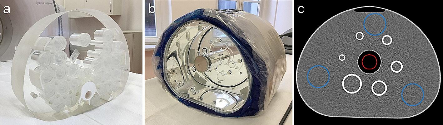
Experimental measurementsReference measurements were made to tune the detector model. A resealable phantom was used, consisting of a cylindrical cavity (20 mm diameter, 8 mm height) with PMMA walls (1 mm top and bottom thickness, 5 mm radial thickness) [11]. Spectra were acquired with the following radionuclides and collimators: \(^}\) (MEGP, LEHR), \(^}}\) (MEGP, LEHR, OPEN) and \(^}\) (MEGP, LEHR, OPEN). A traceable Secondary Standard Dose Calibrator (Southern Scientific, Henfield, United Kingdom) was used to quantify the activity added to the phantom. Measurements were made with the phantom in air to minimise scatter and backscatter, with source-collimator distances of between 25 mm and 150 mm. Figure 1 illustrates the measurement setup.
Fig. 1
Illustration of the measurement setup with the hand-held camera and the cylindrical phantom. The phantom was filled with a magenta dye to visualise the inner cavity
The model was further evaluated by measurements of the system sensitivity as a function of distance for \(^}\) with the MEGP and LEHR collimators. The setup for sensitivity measurements were similar to that of the reference measurements, using source-collimator distances from 0 mm up to 100 mm (MEGP) and 130 mm (LEHR). Energy windows were positioned over 55 keV (49.7 keV to 59.7 keV), 113 keV (100.5 keV to 120.8 keV) and 208 keV (193.8 keV to 216.7 keV), and the total count rates across the full FOV were recorded. For the measured sensitivity, a function was fitted following \(c_0 + c_1 \cdot e^\), where d is the source-collimator distance [34].
CIE map calculationA procedure for calculating CIE maps was implemented in Python using arrays, sparse matrices and linear equation solvers from the NumPy [35] and SciPy [36] packages. The procedure considered a rectangular crystal volume in a Cartesian coordinate system oriented consistently with the convention used by SIMIND. The source-facing side of the crystal was fully covered by a cathode. The opposing side was covered by an array of rectangular anode elements, and the signal generation for one selected anode in this array was considered.
Finite difference approaches [37] were used to numerically estimate the solutions to differential equations 1, 2 and 5. For boundary-value problems (Eqs. 1 and 2), this yielded systems of linear equations which were solved using the loose generalised minimum residual algorithm [38].
The boundary conditions implemented for the differential equations were as follows: For the electric potential (\(\varphi\)), a specified potential difference (600 V) was applied between the anodes and the cathode. The weighting potential (\(\varphi _k\)) was, by definition, calculated with one selected electrode (electrode k) held at a potential of unity and all other electrodes at zero. For charge transport (\(x \in \\)), the condition \(x=0\) was applied on ohmic surfaces and \(\nabla x \cdot } = 0\) was applied on insulating surfaces, where \(}\) is the surface normal [19].
For the inter-anode gaps, the camera’s technical description did not provide sufficient basis for a model implementation of the electrical and weighting potentials. In addition, it was not clear whether the signal contribution from holes was entirely negligible or not. Because of this lack of information, a number of alternative boundary conditions and configurations were implemented (Table 2) and tested as part of the model tuning (“Model tuning” section).
Table 2 Configurations and boundary conditions considered for the CIE calculation procedureFor the electric potential (\(\varphi\)), alternative A1 represented the commonly used assumption of a uniform electric field throughout the crystal [20, 22, 23, 39]. Alternative A2 instead assumed that the electric field lines start and end on electrodes, as expected for ideal dielectric materials [40, 41]. For A2, Eq. 1 was solved with charge density assumed negligible [42]. For imperfect materials with conducting surfaces, a fraction of the field lines may terminate in the inter-anode gaps [40,41,42], as emulated by alternative A3.
For the weighting potential (\(\varphi _k\)) a transition from unity to zero must occur in the gaps between the selected anode and its neighbours. A boundary condition involving the gradient and the surface normal is commonly applied [31, 39, 43, 44], represented by alternative B1. The inverse-distance weighting [45] method (alternative B2) has not been used previously, and was introduced to obtain way to parametrise and adjust the steepness of the lateral sides of the weighting potential and CIE. Additionally, a scale factor was introduced for alternative B2 to force the weighting potential to reach zero at the edge of the neighbouring anode or at some position within the gap, thus allowing for adjustment of the "width" of the anode’s sensitive area. Further details on alternative B2 are given in Additional file 1: Appendix B.
Signal generation from electrons only (C1) or both electrons and holes (C2) were considered. Equation 5 was implemented using a first-order upwinding scheme. The signal integration time was assumed to be long compared to the collection times and the lifetimes of the charge carriers, and the boundary-value problems arising from setting \(\partial x^+/\partial t = 0\) were solved rather than integrating Eq. 5 forward in time.
Due to the periodic pattern of the anode elements, a number of calculated quantities were expected to be symmetric [40, 46, 47]. In particular, this was expected for the electric potential, the weighting potential and the CIE for anode elements near the centre of the detector. For each established plane of symmetry, only one side was considered when solving the equations, and all gradients across were set to zero.
To reduce the computational burden and get manageable calculation times, a compromise was necessary between the extent of the crystal region considered and the spatial discretisation step size. Thus, a \(5 \times 5\) anode element neighbourhood centred around the selected anode was considered instead of the whole crystal, giving a step size of 20 \(}\).
Once all calculations were complete, the CIE map was written to a binary file for later use in the full detector model, including the CIE array, the coordinates associated with the array elements and a selection of parameter values (\(\mu _x,\tau _x\) etc.) for book-keeping.
For consistency control, a CIE map was also calculated without charge diffusion in a parallel-plate geometry (single anode and cathode each covering the entire sides). For this geometry, the electric and weighting fields are uniform. With these conditions, the resulting CIE had a depth-dependence consistent with the Hecht-equation [48].
Monte Carlo simulation of photon interactionsThe SIMIND Monte Carlo program [24] was used to generate sets of realistic photon interactions in the detector crystal. This was made for each of the physical measurements (“Experimental measurements” section). The collimators were simulated with full consideration of the collimator hole geometry and holes were aligned one-to-one with the detector anodes, to properly model the decreased likelihood of interactions above the gaps between the anodes. This collimator effect is visible in Fig. 2. Each photon interaction in the detector crystal was logged in a listmode format, including information about the interaction type (photoelectric absorption, Compton scatter, elastic scatter), interaction coordinates, deposited energy and variance-reduced photon weight [49]. The events originating from different photon histories were recorded as separate entries in the listmode file.
Fig. 2
A Volume rendering of a CIE map (\(\eta _k\)). B Cross section of a CIE map with photon interaction positions from SIMIND overlaid as black points. The collimator septa (MEGP) are indicated at the bottom, and the decreased probability for interactions behind them can be noted. Dotted lines indicate the lateral centres of the anode gaps
Full detector modelA detector model mimicking the hand-held camera system was implemented in IDL (Interactive Data Language, Harris Geospatial Solutions Inc.). The basic building blocks were individual anode elements, which processed events separately from one-another. A CIE map (\(\eta _k\)) was associated to each element, and was defined according to
$$\begin \eta _k(\mathbf ) = \eta _\mathrm (\mathbf + \mathbf _k-\mathbf _\mathrm ), \end$$
(6)
where \(\eta _\mathrm \) was generated using the procedure in “CIE map calculation” section. This joint CIE map, implemented in the form of a discrete three-dimensional array, was calculated for a central anode element (\(\mathbf _k = \mathbf _\mathrm \)). The associated maps for all other anode elements (\(\mathbf _k \ne \mathbf _\mathrm \)) were determined by applying suitable translations (Eq. 6). The full detector model was obtained by creating a \(16 \times 16\) array of individual anode elements.
The model used the listmode files generated by SIMIND as input. For each photon history H, the total response \(E_,k}\) for each anode element k was calculated according to
$$\begin E_,k} = \sum _ \eta _k\left( \mathbf _i\right) \cdot E_i, \end$$
(7)
where i denotes an individual photon interaction event for which the energy \(E_i\) is deposited at a point \(\mathbf _i\). Tri-linear interpolation within the CIE array was used to evaluate \(\eta _k\left( \mathbf _i\right)\). This coupling between a calculated CIE map and interactions from SIMIND is illustrated in Fig. 2.
Following Eq. 7, each photon history yielded 256 separate energy-responses \(E_,k}\) (one per anode element). Due to photon scattering and charge sharing, the response was not limited to a single anode [50]. Generally one or a few anodes produced substantially higher values of \(E_,k}\) than others. As the technical specifications of the detector module indicated that only one anode registers a count per impinging photon, a post-processing step was included in which the anode with the largest value of \(E_}\) was assigned to win the photon history, while \(E_,k}\) from all other anodes were discarded. The signal from the winning anode was used to record a count (scaled by the photon weight) in the energy spectrum. These initial spectra did not incorporate any energy resolution effects beyond the photopeak widening caused by the low-energy tails. Furthermore, as \(\eta _k\) had values below unity (\(\eta _k < 0.9\) in Fig. 2), the photopeaks tended to shift downwards. To take these factors into account, two subsequent steps were applied. In the first step, the spectrum was re-sampled according to a linear energy-calibration:
$$\begin E_} = a_0 + a_1 \cdot E_}, \end$$
(8)
where \(E_}\) was the energies of the uncalibrated spectrum, and \(E_}\) were the new energies calculated such that the photopeaks were aligned with the corresponding photon emission energies. The second step aimed at mimicking additional energy resolution effects by applying a Gaussian smoothing with an energy-dependent full width at half maximum (FWHM), as given by:
$$\begin \mathrm (E) = b_0 + b_1 \cdot E. \end$$
(9)
Application of Eq. 8 mimics the calibration of energy-versus-channel number used by the camera manufacturer [3]. The linear function for the FWHM (Eq. 9) was used based on the findings in Roth et al. [11].
Because the application of the energy resolution had a small effect on the peak positions, an iterative procedure was developed in which the parameters of the energy calibration (Eq. 8) were solved for given values of the energy resolution parameters (Eq. 9). Thus, the parameters \(a_0,\) and \(a_1\) were determined such that the photopeaks would be correctly placed after the energy resolution step (for details, see Additional file 1: Appendix C).
Energy spectra were recorded for individual anode elements in a format identical to that of the camera (“The hand-held camera” section). This format allowed spectra to be formed by adding the spectra from selected anode elements. With the anode element arrangement known, image formation was achieved by integrating all counts within a given energy-window for each individual anode-spectrum. In addition, information provided in the simulation listmode files allowed the spectra to be divided into components based on the photon classification (primary, scatter, penetration etc.) and original emission energy.
Model tuning“The hand-held camera” section lists specifications and parameters known for the camera and its detector module. Beyond these, other parameters such as charge mobilities, charge lifetimes, and the shapes of the electric and weighting potentials, were not known with precision. The crystal properties are known to vary throughout manufactured CZT ingots [51], and a relatively wide range of mobilities and lifetimes for electrons and holes has been reported in the literature [8, 30, 44, 52,53,54]. A further complication was that the features of the CIE map (\(\eta _\mathrm \)) and the energy resolution were not independent of each other, since the magnitude of the low-energy tails were governed by the CIE map, and in turn, these tails contributed to the energy resolution. Consequently, experimentally determined energy resolution functions [11] were not directly applicable.
Because of these factors, tuning of the parameter values and boundary conditions was required, with the goal of obtaining a detector model capable of replicating the experimental measurements as closely as possible. To take the large amount of experimental measurements (“Experimental measurements” section) and adjustable parameters into account simultaneously, the parameter tuning was performed as an automated procedure, illustrated in Fig. 3.
Fig. 3
A Flow-chart of the model tuning procedure. B Example of an initial spectrum, and results after applying the energy correction and energy resolution. C Comparison against measured spectrum
The different CIE settings listed in Table 2 were combined, and together yielded eight basic CIE configurations (Additional file 1: Appendix D). The parameter tuning procedure was executed separately for each of these configurations. In each run, the values of the configuration-associated parameters (Additional file 1: Appendix E) were optimised (outer loop in Fig. 3). Given a set of parameter values, a CIE map (\(\eta _\mathrm \)) was generated. For each radionuclide-collimator combination, the Monte Carlo simulated photon interactions were processed with this CIE map to form an initial spectrum (Eq. 7), the energy calibration parameters were determined, and the energy calibration and resolution applied. The energy resolution parameters were optimised separately from the CIE parameters (inner loop in Fig. 3), as the generation of a new CIE map was by far the most time-consuming step. The same energy calibration was used for all simulated spectra, and was determined using the simulation of \(^}\) and MEGP. To enable direct comparison of measured and simulated spectra, energy calibration was also made for the measured spectra to ensure consistent photopeak positioning, which otherwise varied slightly depending on the detector temperature at measurement [11,
留言 (0)